Chemical Vapor Deposition (CVD): Principles, Uses and Developments Guide
Chemical Vapor Deposition (CVD) is a manufacturing and materials-processing technique used to create thin, solid layers on the surface of a material.
During CVD, one or more chemical compounds are introduced into a controlled chamber, where heat or another form of energy causes them to react or break down. The resulting solid material forms a coating or thin film on a selected surface.
CVD has roots in early chemical and metallurgical research involving vapor-phase reactions. As vacuum technology, controlled atmospheres, and materials science developed, the technique became increasingly useful for producing controlled coatings. Modern CVD is widely associated with semiconductor manufacturing, advanced materials, cutting tools, optical components, energy technologies, and laboratory research.
How Chemical Vapor Deposition Works
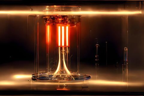
A typical CVD system contains a reaction chamber, gas delivery equipment, a substrate holder, heating equipment, pressure controls, and an exhaust or gas-treatment system. The substrate is the material on which the new layer is deposited.
The basic sequence generally includes:
- Preparation of the substrate surface
- Introduction of precursor gases into the chamber
- Activation of chemical reactions through heat, plasma, light, or another energy source
- Formation of reactive species
- Chemical reaction at or near the substrate
- Growth of a solid film
- Removal of gaseous reaction products
The exact chemistry depends on the material being deposited. Silicon, silicon carbide, silicon nitride, titanium compounds, carbon-based materials, and various metal-containing films can be produced using different CVD approaches.
Major Types of CVD
Several CVD methods have been developed for different materials and temperature requirements. Thermal CVD uses heat to activate chemical reactions, while plasma-enhanced CVD uses plasma to promote reactions at comparatively lower substrate temperatures.
Other approaches include low-pressure CVD, atmospheric-pressure CVD, metal-organic CVD, and hot-filament CVD. Each method changes factors such as pressure, precursor chemistry, energy input, deposition rate, and film properties.
| CVD Method | Main Characteristic | Typical Applications |
|---|---|---|
| Thermal CVD | Heat-driven chemical reactions | Ceramic and semiconductor films |
| Low-Pressure CVD | Reduced chamber pressure | Silicon-based coatings |
| Plasma-Enhanced CVD | Plasma activates reactions | Electronics and protective films |
| Metal-Organic CVD | Uses metal-organic precursors | Compound semiconductors |
| Hot-Filament CVD | Heated filament activates gases | Diamond and carbon films |
Importance
Chemical Vapor Deposition matters because thin surface layers can change how a material behaves without requiring the entire component to be made from the deposited material. A carefully controlled coating can provide electrical, optical, thermal, chemical, or mechanical characteristics suited to a particular application.
Role in Electronics and Semiconductors
The semiconductor industry uses CVD to create thin layers that form part of electronic structures. Materials deposited through CVD can act as conductors, insulators, barriers, protective layers, or components of semiconductor devices.
The ability to control film thickness and composition at small scales is important for integrated circuits, sensors, memory technologies, and other electronic components. Manufacturing environments may combine CVD with lithography, etching, cleaning, polishing, and other fabrication techniques.
Industrial and Engineering Applications
CVD coatings are also used in applications where surface properties are important. Cutting tools, mechanical components, optical parts, and high-temperature materials can use deposited layers to modify surface behavior.
Applications include:
- Wear-resistant coatings for selected industrial components
- Protective layers for high-temperature materials
- Semiconductor and electronic structures
- Optical coatings and specialized components
- Carbon and diamond-related materials
- Solar and energy-related technologies
- Research into advanced ceramics and functional materials
Control of Film Properties
CVD allows researchers and engineers to adjust several characteristics by changing operating conditions. Important parameters include temperature, chamber pressure, gas composition, precursor concentration, gas flow, reaction time, and substrate condition.
Small changes in these parameters can influence film thickness, grain structure, chemical composition, surface roughness, adhesion, and electrical characteristics. For this reason, monitoring and process control are important parts of CVD operation.
Recent Updates
Recent developments in Chemical Vapor Deposition have focused on improving process control, reducing unwanted reactions, supporting advanced materials, and integrating deposition equipment with digital manufacturing systems.
Lower-Temperature Deposition
Research continues to develop CVD approaches that can deposit useful films at lower temperatures. Lower-temperature processing can be relevant when the underlying substrate cannot tolerate high heat or when multiple materials must be integrated within a device.
Plasma-enhanced techniques and other activation methods can help initiate chemical reactions under conditions different from conventional thermal CVD.
Advanced Semiconductor Materials
CVD remains important in research and manufacturing involving compound semiconductors, wide-bandgap materials, and other electronic materials. Silicon carbide and related materials have received attention because of their role in power electronics and high-temperature applications.
Metal-organic CVD is also used for compound semiconductor structures where precise control of material composition and layer thickness is required.
Automation and Digital Monitoring
Modern CVD equipment increasingly incorporates sensors, automated gas control, pressure monitoring, temperature measurement, and software-based process records. These systems can help operators observe changes in chamber conditions during deposition.
Data analysis is also being used to identify relationships between process parameters and film characteristics. Machine learning research is being explored for process modeling, equipment monitoring, defect identification, and parameter optimization.
Advanced Carbon Materials
CVD techniques continue to play a role in producing graphene, carbon nanotubes, diamond films, and other carbon-based structures. Research focuses on controlling nucleation, crystal structure, layer thickness, surface morphology, and material purity.
These developments are relevant to electronics, thermal management, sensing, energy research, and specialized engineering applications.
Laws or Policies
In India, Chemical Vapor Deposition activities can involve several areas of regulation because the process may use hazardous chemicals, pressurized gases, high temperatures, vacuum equipment, electrical systems, and industrial exhaust.
Workplace Safety
Industrial workplaces are subject to occupational safety requirements under India's broader workplace and industrial safety framework, including provisions associated with the Occupational Safety, Health and Working Conditions Code, 2020. Actual requirements depend on the facility, workforce, chemicals used, and applicable implementation rules.
CVD facilities generally need appropriate controls for gas handling, ventilation, chemical exposure, pressure systems, electrical equipment, emergency procedures, and worker training.
Environmental Requirements
The Ministry of Environment, Forest and Climate Change, Central Pollution Control Board, and relevant State Pollution Control Boards have responsibilities related to environmental protection and industrial emissions.
Facilities using chemical precursors and generating gaseous reaction products may need environmental controls appropriate to their operations. Requirements can vary according to the facility, materials, emissions, location, and applicable permissions.
Standards and Technical Guidance
Bureau of Indian Standards publications and international standards may be relevant to equipment safety, electrical systems, laboratory practices, materials testing, and industrial measurement. Chemical handling practices should also follow applicable safety data sheets and institutional procedures.
Because CVD systems can differ substantially, the applicable regulatory requirements should be determined from the specific process, chemicals, equipment, and facility classification.
Tools and Resources
Understanding or operating Chemical Vapor Deposition requires several categories of equipment and reference material.
Process Equipment
Common equipment includes:
- Reaction chambers
- Vacuum pumps and pressure controllers
- Mass flow controllers
- Gas cylinders and delivery systems
- Heating systems
- Plasma generators for plasma-based methods
- Temperature sensors
- Pressure gauges and sensors
- Exhaust treatment equipment
Gas delivery systems regulate precursor and carrier gases. Pressure-control equipment maintains the required chamber environment, while temperature measurement helps maintain repeatable deposition conditions.
Film Characterization Tools
After deposition, the resulting film can be examined using different analytical techniques. Profilometry can measure film thickness, while scanning electron microscopy can provide information about surface structure and cross-sectional features.
Other commonly used techniques include X-ray diffraction for structural analysis, Raman spectroscopy for selected materials, ellipsometry for thin-film measurements, atomic force microscopy for surface characterization, and electrical testing for conductive or semiconductor films.
Reference Resources
Useful technical resources include publications from the Bureau of Indian Standards, Central Pollution Control Board, National Physical Laboratory, CSIR laboratories, and international standards organizations. Academic journals and university materials science resources can also provide information about deposition chemistry, equipment design, and thin-film characterization.
FAQs
What is Chemical Vapor Deposition?
Chemical Vapor Deposition is a technique for producing a solid thin film on a substrate through chemical reactions involving vapor-phase precursor materials. Controlled temperature, pressure, gas flow, and chemical composition influence the resulting layer.
How does Chemical Vapor Deposition work?
Chemical Vapor Deposition introduces selected precursor gases into a controlled chamber. Energy activates chemical reactions, and the resulting solid material forms a layer on the substrate while gaseous reaction products are removed.
What materials can be deposited using CVD?
CVD can produce various materials, including silicon-based compounds, silicon carbide, silicon nitride, carbon materials, diamond films, metal compounds, and selected semiconductor materials. The available materials depend on precursor chemistry and the specific CVD method.
What is the difference between thermal CVD and plasma-enhanced CVD?
Thermal CVD primarily relies on heat to activate chemical reactions. Plasma-enhanced CVD uses plasma energy to activate or accelerate reactions, which can allow deposition under different temperature and process conditions.
Where is Chemical Vapor Deposition used?
Chemical Vapor Deposition is used in semiconductor manufacturing, electronics, optical components, cutting tools, advanced ceramics, energy technologies, carbon materials, and research laboratories. Its applications depend on the properties required from the deposited film.
Conclusion
Chemical Vapor Deposition is a thin-film manufacturing technique based on controlled chemical reactions between vapor-phase materials and a substrate. It has become important in electronics, semiconductor technology, industrial coatings, optical components, energy research, and advanced materials. Current developments emphasize lower-temperature processing, improved process monitoring, automation, advanced semiconductor materials, and carbon-based structures. Safe operation requires appropriate control of chemicals, gases, temperature, pressure, emissions, and workplace conditions.

Related Post...
Chemical Vapor Deposition (CVD): Principles, Uses and Developments Guide
Updated: September 10, 2026
Read More
Industrial Laser Annealing: Explore Basics, Equipment, Methods, and Applications
Updated: September 09, 2026
Read More
Industrial Incinerators: Insights Into Waste Treatment, Emissions, Safety, and Operation
Updated: September 09, 2026
Read More